Sparkgap
Reading time : 1 minute
Published on 16 Jun 2020 - Updated on 09 Mar 2021
Sparkgap is the cheapest way to do an ESD protection on a PCB without any component. It works very simple, it uses the fact that if voltage is too high it will produce a spark and short the two conductors together.
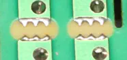
Here are some examples of sparkgaps designed on PCB :


Design tips
- Place the sparkgap as close as possible to connectors or where ESD can occur. ESD Wave has to be shorted to ground as soon as possible.
- Remove coating on the sparkgap. Only plating and copper should remain.
- 0.2mm space is a good basic spacing value
Formula
$$ V=\frac{3000 \times P \times D}{1000}+1350 $$\( V \) is voltage that will cause a spark in Volts
\( P \) is the atmospheric pressure in hectopascal (usually 1013 hPa)
\( D \) is distance in millimeters
As a rule of thumb : 0.2mm space gives you approximately 2kVolts due to PCB tolerances and atmospheric pressure variation.

